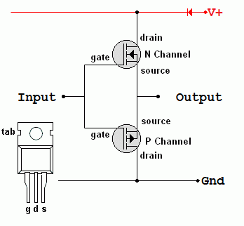
MOSFET Push Pull Amplifier |
|
To gain access to revision questions, please sign up and log in.
a
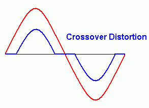
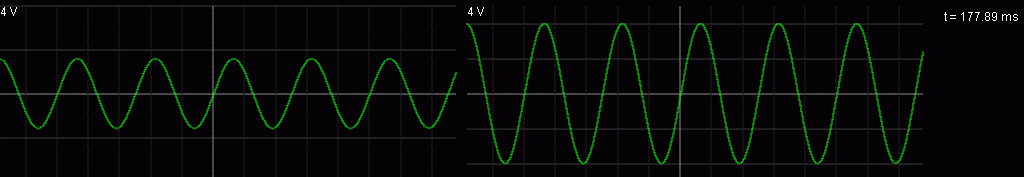
This simple circuit suffers from cross over distortion.
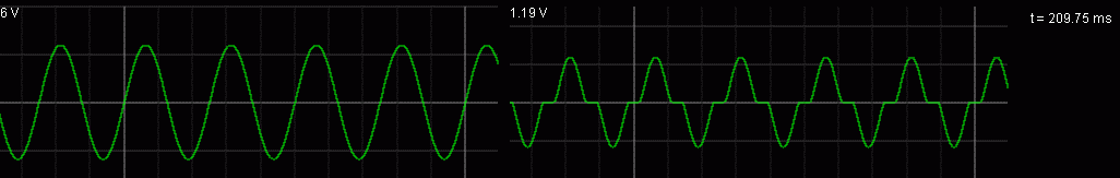
The red trace is the input signal. The blue trace is the output.
 |
 |
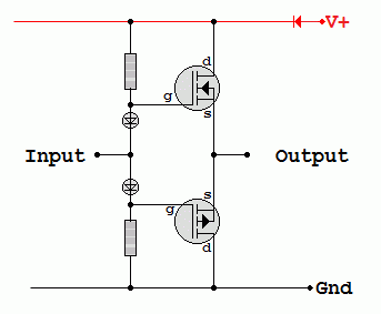
This diagram shows simple biasing using diodes and resistors. 0.7 Volts is lost across the diodes so the output will be lower than expected compared with using ideal components. It is possible to use LEDs. In this case about two Volts will be lost.
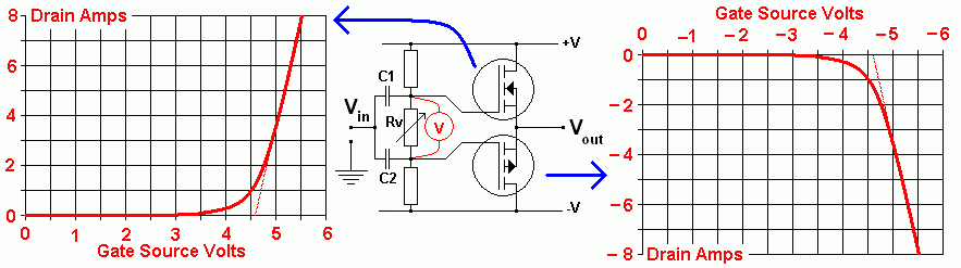
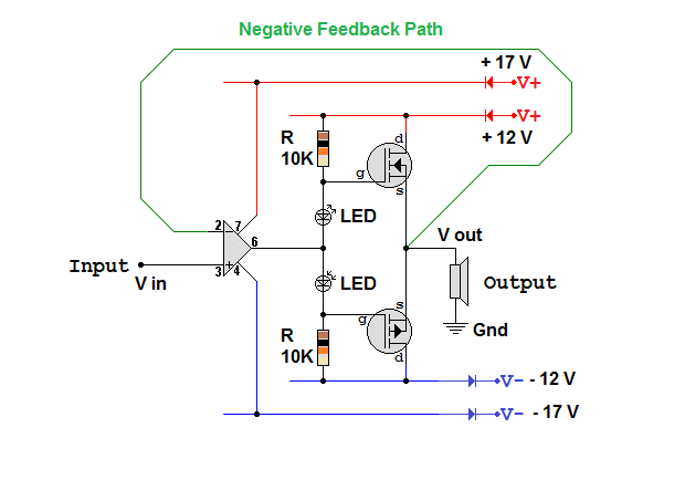
The diagram below is similar but has adjustable biasing. The additional voltage divider resistors, with Rv adjustable are chosen so that both MOSFETS are just on the point of turning on. Rv is adjusted to give a small quiescent current (the current flowing when there is no input signal).
Looking at the graphs, the N Channel MOSFET needs about +3.5V to just start it conducting. The P Channel MOSFET needs -3.5V. The potential difference measured by the voltmeter will be 7 Volts.
Coupling capacitors are needed to get the AC input to the MOSFET gates at the same time as blocking the DC bias voltages. This circuit can not be used to amplify DC signals.
Diodes could be included with the biasing resistors. These would improve the thermal stability of the circuit by tending to shut down an overheating circuit.
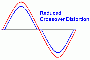 The red trace is the input signal. The blue trace is the output. The distortion is reduced.
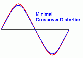
The red trace is the input signal. The blue trace is the output. The distortion has gone.
 |
 |
This push-pull amplifier uses a voltage follower and MOSFET biasing. It runs on + and - 12 Volts and is similar to the diagram above.
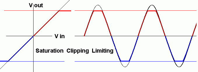
The image below shows ideal (black) and non-ideal (red and blue) behaviour including clipping when the op amp is saturated and the output voltage can go no higher.
Amplifiers of any type can not produce output voltages that are larger than the power supply voltages. If the input is too big, the amplifier output will increase until it is nearly equal to the supply voltage. After that the output voltage can not rise any more. The black line shows the amplifier input signal. The red line shows the output from the N Channel MOSFET. The blue line shows the output from the P Channel MOSFET.
Vrms = 0.7 x Vpeak
Power = Vrms2 / R
Power = (20 x 0.7)2 / 8
Power = 24.5 Watts
This is the theoretical maximum power output.
kIn real life, MOSFET push pull source followers are not perfect. The output will be lower than expected because ...
Points 1 to 3 above can be fixed by running the op-amp driver and MOSFET biasing on a higher power supply voltage. As these are low power circuits, this is not too expensive to do.
l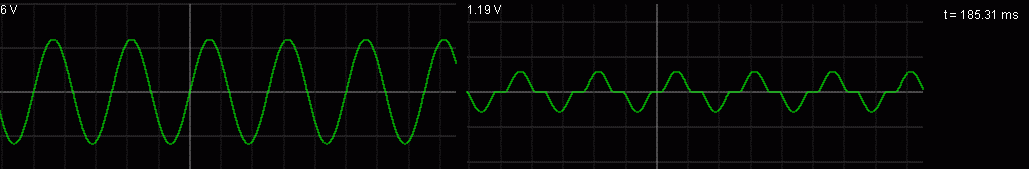
For the Falstad Circuit Simulation, CTRL+Click Push Pull Source Followers with no Bias and no Negative Feedback
In options, check European Resistors and uncheck Conventional Current.
Alternatively view Push_Pull_No_Bias_No_Feedback.txt.
Save or copy the text on the web page. Import the saved or copied text into the Falstad simulator.
Here is the new HTML5 Simulator Site.
For the Falstad Circuit Simulation, CTRL+Click Push Pull Source Followers with Bias but no Negative Feedback
In options, check European Resistors and uncheck Conventional Current.
Alternatively view Push_Pull_Bias_No_Feedback.txt.
Save or copy the text on the web page. Import the saved or copied text into the Falstad simulator.
Here is the new HTML5 Simulator Site.
For the Falstad Circuit Simulation, CTRL+Click Push Pull Source Followers with Bias and Negative Feedback
In options, check European Resistors and uncheck Conventional Current.
Alternatively view Push_Pull_Bias_Feedback.txt.
Save or copy the text on the web page. Import the saved or copied text into the Falstad simulator.
Here is the new HTML5 Simulator Site.
This can be eliminated by using a higher power supply voltage as long as all the components can handle this and also the extra waste heat produced.
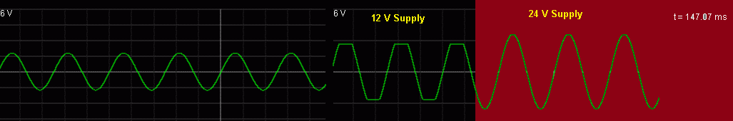
For the Falstad Circuit Simulation, CTRL+Click Overloaded Push Pull Source Followers
In options, check European Resistors and uncheck Conventional Current.
Click both the switches to double the power supply voltage.
Alternatively view Saturation.txt.
Save or copy the text on the web page. Import the saved or copied text into the Falstad simulator.
Here is the new HTML5 Simulator Site.
reviseOmatic V3 Contacts, ©, Cookies, Data Protection and Disclaimers Hosted at linode.com, London