Audio Amplifiers |
|
To gain access to revision questions, please sign up and log in.
|
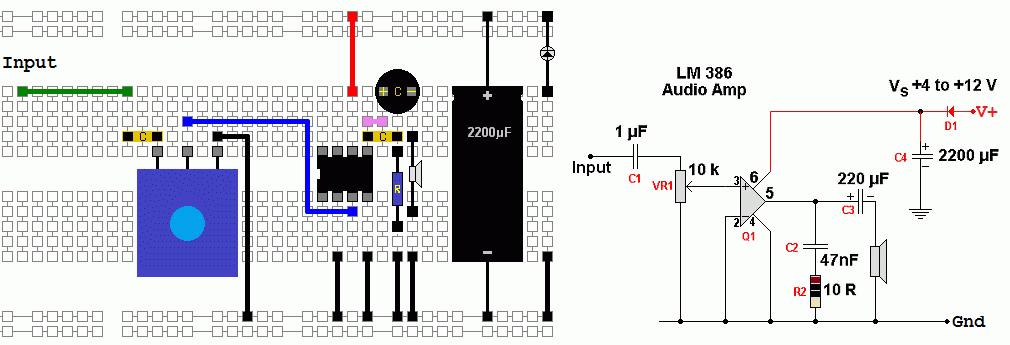
Many chips and modules are available. This makes it easy to build an audio power amplifier subsystem. |
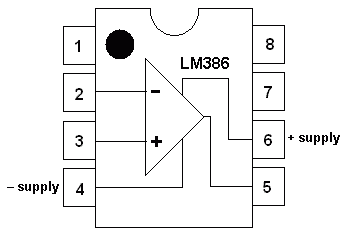
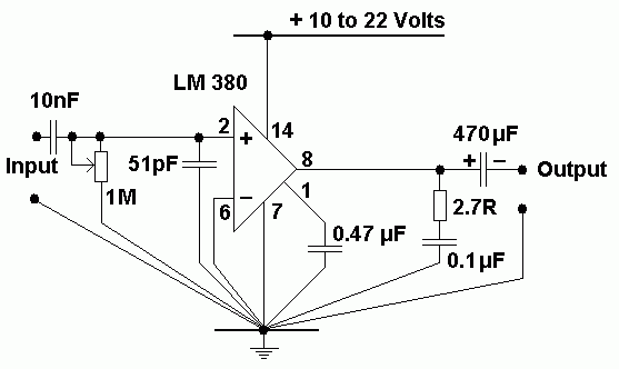
This chip is ideal for portable low voltage circuits like small radios. No heatsink is needed.
|
Connecting all the zero volt wires as close together as possible is called single point earthing or grounding. This reduces mains hum and the chances that the circuit will oscillate unexpectedly. With this low power amplifier, it's not really necessary but it's essential with higher powered circuits. LM386 Details
|
Output Power = Vrms2 / R
Vrms = 0.7 Vpeak
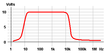
The Voltage BANDWIDTH of an amplifier is defined as the range of frequencies where the output voltage is at least 0.7 or 70% of the maximum output.
The Power BANDWIDTH of an amplifier is defined as the range of frequencies where the output power is at least 0.5 or 50% of the maximum output.
This image shows a bandwidth going from 10Hz up to about 20 kHz giving a 19990 Hz bandwidth which rounds off to 20 kHz.
The output should be identical to the input but at a higher voltage or current. Most circuits come close to this ideal but are not perfect. The damage to the output signal is called distortion. If is often expressed in percent.
Not as easy to build this circuit as the lower power LM386 above.
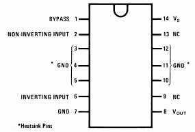
Another Audio Power Amplifier IC
For safe operation and full output power, this chip needs to be bolted onto a fairly large heat sink.
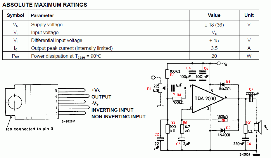
This is an extract from an S T Microelectronics data sheet. The device provides 8 to 14 Watts of audio depending on the power supply voltage and the load resistance.
Higher supply voltages give larger power outputs. This is a square law so doubling the supply gives four times the power.
Keeping the device cool is critical. It has thermal shutdown which will limit the output power if it becomes too hot. A good heat-sink needs to be used.
R1 |
is a potentiometer used as a volume control. It also determines the input resistance of the sub-system. |
|
R2 and R3 |
form a voltage divider providing half the power supply. |
|
C2 |
is a decoupling capacitor. It ensures that the halved power supply voltage is steady and free from any AC signal. |
|
R4 |
holds the non inverting input at a DC level equal to half the power supply voltage. |
|
C1 |
is a coupling capacitor. It couples the audio input to the non inverting pin of the amplifier. It also blocks the DC voltage between the audio input and the chip. |
|
C4 and C5 |
are decoupling capacitors. Two are needed because the C4 performs well at low frequencies but badly at high frequencies. C5 performs well at high frequencies but not at low ones. Between them they decouple the full range of frequencies. |
|
TDA2030 |
This is the audio amplifier Integrated Circuit (IC). It is similar to an ideal op-amp but it provides a much higher power output. |
|
R5 and R6 |
control the gain of the amplifier. It is a non inverting amplifier and the gain is found from 1 + R6 / R5. |
|
C3 |
is a decoupling capacitor. It grounds AC signals so the chip works as a normal non inverting amplifier for AC signals. It leaves a DC feedback path so the chip's DC levels are well controlled. |
|
D1 and D2 |
prevent the output going above the DC + supply or below the DC - supply. This protects the chip from back emf voltage spikes caused by driving an inductive load. (Some speaker systems contain cross-over filter circuitry containing inductors.) |
|
C7 |
is a coupling capacitor. It couples the audio output to the loudspeaker and blocks the DC level which would otherwise destroy the speaker. |
|
C6 and R7 |
This is an equalisation circuit. Without this the amplifier would probably oscillate at a high frequency, perhaps inaudible, but likely to damage the speaker or tweeter if there is one. |
reviseOmatic V3 Contacts, ©, Cookies, Data Protection and Disclaimers Hosted at linode.com, London