WANTED: Individual or team to take over this project. I'm in my 70's and want to put my feet up. Contact details in footer.
| A Level Semiconductor >Photodiode< |
Semiconductor Photodiode |
|
This is a reverse biased diode. When exposed to light, the diode reverse leakage current increases greatly. Energetic photons dislodge charge carriers from their silicon parent atoms. These charge carriers (electrons and holes) flow and the leakage current depends on the light level.
Photodiodes respond very much faster than light dependent resistors.
PIN Diodes are the fastest of all and are used to detect light emerging from optical fibres in communication systems.
PIN Diodes are used as photo detectors and for high frequency radio switches and attenuators.
The diode has three layers.
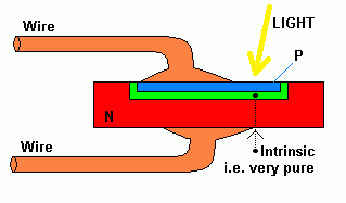
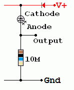
When the device is reverse biased, there is a minute leakage current. If light (photons) hit the Intrinsic Layer, electrons are dislodged and this leaves a hole. The electrons migrate towards the Anode (positive) and the holes migrate towards the Cathode (negative). So light shining on the device increases the leakage current.
If the PIN diode is reverse biased with a very high voltage, when an electron is dislodged, it accelerates towards the anode and this dislodges more electrons which also accelerate. This causes an avalanche effect and quite a large current pulse flows even if only one photon triggered the avalanche.
Ten gigabits per second data transfer rates are possible because these diodes respond so fast.
Diode Characteristics ...
|
5nA |
|
|
1.2 A/W |
1.2 amps per Watt. So 1 microwatt of light would produce a leakage of 1.2 microamps. |
|
8pF |
Reverse biased diodes behave like capacitors. Between the P and N layers there is s depletion zone where there are no charge carriers. So there are two conducting zones separated by an insulating zone. This structure is just like a capacitor. It gets more interesting. As the reverse bias is increased, the depletion zone gets bigger so the capacitance decreases. It's like increasing the plate separation of a capacitor. |
|
5nS |
As the diode also behaves like a capacitor, this circuit behaves like an RC timing circuit. This limits the speed at which the diode can switch. A smaller capacitance increases the switching speed. A higher reverse bias voltage reduces the capacitance. The breakdown voltage must not be exceeded. |
|
|
Dark Output VoltageUse the dark leakage current for this calculation. V = I R = 5x10-9 x 2.2x106 = 11mV Vout at 2µWatts Incident LightThe diode produces 1.2 Amps per Watt or 1.2 microamps per microwatt to the current will be just over 2 µA. I = 5x10⁻⁹ + 2x10-6 x 1.2 = 2.405µA V = I R = 2.405x10-6 x 2.2x106 = 5.29 V RC Time Constant at Zero BiasT = R C = 2.2x106 x 8x10-12 = 17.6 µs The PIN diode responds much faster than this because it is not used at zero bias. The highest possible reverse bias is used. This greatly reduces the capacitance of the device. Circuit SensitivityTo increase the sensitivity ...
|
Contact, Copyright, Cookies and Legalities: C Neil Bauers - reviseOmatic V4 - © 2016 to 2026
Hosted at Akamai Cloud - London
Please report website problems to Neil