PIC16F88 0C ADC Input |
|
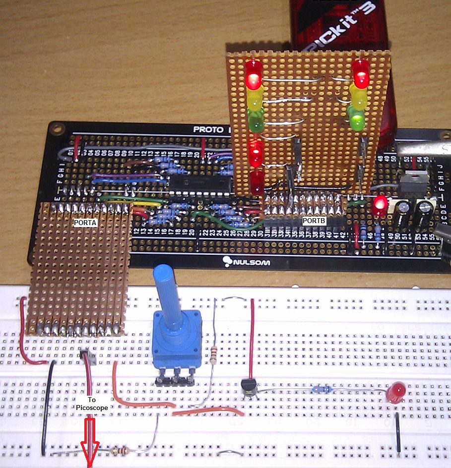
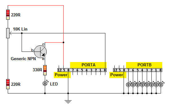
This circuit provides an analogue voltage to test the ADC function on the PIC16F88, plugged into PORTA, pin AN0/RA0.
The 220R resistors prevent potentiometer destruction if it's mis-wired.
It's OK to use a log pot if a linear one is not available.
The optional transistor and LED give a visual indication of the analogue voltage from close to 0 up to nearly 5Volts.
There are 8 LEDs, used to show the binary ADC output, plugged into PORTB.
Their 330R current limiting resistors are build onto the PIC16F88 board and not shown here.
The program repeatedly reads the ADC or potentiometer position and copies the value to the LEDs.
It's a 10 bit ADC. To show the result on the eight LEDs, the two least significant bits are discarded.
The accuracy drops from 1 part in 1024 to 1 part in 256. For a quick demonstration, this is not a problem.
For many applications this accuracy level would be more than enough. It's better than 1%. Most components are not that accurately manufactured.
With a 4 MHz clock, the chip managed over 17 000 conversions per second. This would be sufficient for good quality audio but not full frequency range HiFi.
;*******************************************************************************
; PIC16F88 Configuration Bit Settings
;*******************************************************************************
#include "p16F88.inc"

; CONFIG1: Internal RC Oscillator with I/O on RA6 and RA7. Turn of everything else.
 __CONFIG _CONFIG1, _FOSC_INTOSCIO & _WDTE_OFF & _PWRTE_OFF & _MCLRE_OFF & _BOREN_OFF & _LVP_OFF & _CPD_OFF & _WRT_OFF & _CCPMX_RB0 & _CP_OFF

; CONFIG2: Allow Fail Safe Clocking. Turn off internal/external clock choice
 __CONFIG _CONFIG2, _FCMEN_ON & _IESO_OFF

;*******************************************************************************
; Uninitialised Data - Reserve bytes here ...
;*******************************************************************************
	    UDATA
ADC_Result  RES	    1	    ; reserves 1 byte for the ADC result
Del_Count   RES	    1	    ; used in the delay loop

;*******************************************************************************
; RESET VECTOR
;*******************************************************************************
RES_VECT    CODE 0x0000	    ; processor reset vector
    GOTO    CODE_INIT	    ; beginning of program, initialise stuff

;*******************************************************************************
; INTERRUPT HANDLING
;     This ought to save and restore the context
;     It's not secessary in this simple example
;*******************************************************************************
ISR CODE    0x0004	    ; The interrupt vector location is always 0x0004
    BCF	    INTCON, GIE	    ; Prevent the interrupt from being interrupted

    BANKSEL ADRESH
    MOVF    ADRESH, 0	    ; Copy the 8 most significant ADC bits to WREG

    BANKSEL PORTB
    MOVWF   PORTB	    ; Copy WERG to PORTB to show ADC result on LEDs

    MOVLW   b'11011110'	    ; to invert PORTA outputs but not RA5 or RA0
    XORWF   PORTA, 1	    ; The PORTA bits are inverted so the conversion
			    ; rate can be measured on an oscilloscope

    CALL    ADC_START	    ; Start the next conversion
    RETFIE		    ; Return from interrupt


;*******************************************************************************
; MAIN PROGRAM - CODE INITIALISATION
;*******************************************************************************
MAIN_PROG   CODE	    ; let linker place main program

CODE_INIT:		    ; INITIALISATION
    CALL    CLOCK_INIT	    ; Set the clock frequency
    CALL    PORT_INIT	    ; Set up I/O Port Directions
    CALL    ADC_INIT	    ; Set up A to D Converter
    CALL    ADC_START	    ; Start the ADC and wait for the completion interrupt.
    GOTO    IDLE_LOOP	    ; Jump to the Infinite Idle Loop - wait for interrupts

;*******************************************************************************
; INITIALISE CLOCK FREQUENCY - 4MHz - 1 microsecond per instruction
;*******************************************************************************
CLOCK_INIT:
    BANKSEL OSCCON
    movlw   b'01100000'	    ; -110----    4 MHz
    movwf   OSCCON	    ; At 4 MHz it's one microsecond per line of code.
    RETURN

;*******************************************************************************
; INITIALISE PORTS
;*******************************************************************************
PORT_INIT:
    BANKSEL TRISA
    MOVLW   b'00000001'	    ; Six Outputs. RA0/AN0 will be an analogue input. RA5 is always an input.
    MOVWF   TRISA	    ; Set PORTA data directions.
    MOVLW   b'00000000'	    ; Eight output lines for the eight LEDs
    MOVWF   TRISB	    ; Set PORTB data directions.

    BANKSEL PORTA
    MOVLW   0x00	    ; Clear PORTA and PORTB
    MOVWF   PORTA
    MOVWF   PORTB

    RETURN

;*******************************************************************************
; INITIALISE ADC
;*******************************************************************************
ADC_INIT:
    BANKSEL ANSEL
    MOVLW   b'00000001'	    ; AN0 will be an analogue input. This is same pin as RA0.
    MOVWF   ANSEL	    ; Set Analogue Select Register

    BANKSEL ADCON1
    MOVLW   b'00000000'	    ; Set up ADCON1
;             ||||3210------- Not used
;             ||54----------- Use power supply lines as voltage references
;             |6------------- Don't divide AtoD clock source by 2 - ADCS2
;             7-------------- Left justify the result bits. Use ADRESH and discard the two bits in ADRESL
    MOVWF   ADCON1	    ; Save settings to A to D Control Register 1

    BANKSEL ADCON0
    MOVLW   b'01000001'	    ; Set up ADCON0    0xC1
;             |||||||0-------   1 Turn on the ADC - ADON
;             ||||||1--------     not used
;             |||||2---------   0 set this to one to start a conversion
;             ||543---------- 000 selects channel 0, RA0/AN0
;             76-------------  01 divides 4MHz clock by 8   0.25us * 8  =  2 us  OK because the safe range is 1.6 to 6.4 us
    MOVWF   ADCON0	    ; Save settings to A to D Control Register 0

    RETURN

;*******************************************************************************
; START ADC
;*******************************************************************************
ADC_START:
    BANKSEL PIE1
    BSF	    PIE1,   ADIE    ; Set A to D Interrupt Enable in the peripheral interrupt register

    BANKSEL PIR1
    BCF	    PIR1,   ADIF    ; Clear A to D Interruot flag in Peripheral interrupt register
    BSF	    INTCON, PEIE    ; Turn on Peripheral Interrupts
    BSF	    INTCON, GIE	    ; Turn on Global Interrupts

    MOVLW   d'1'	    ; Delay d'1' * 4 + 2 + 2  =~  8 microseconds
    CALL    DELAY_W	    ; Should be enough for the sample and hold to work

    BANKSEL ADCON0
    BSF	    ADCON0, GO	    ; Set the ADC GO bit - Start the AD Converter
    RETURN

;*******************************************************************************
; The Idle Loop
; MS Windows has an "idle process" which waits for the user to do something.
;*******************************************************************************
IDLE_LOOP:
    NOP
    NOP	; NOPs make the code execution obvious in the simulator
    NOP	; Leave them out in real life
    NOP
    GOTO    IDLE_LOOP


;*******************************************************************************
; 200 microsecond delay at 4MHz clock
;*******************************************************************************
DELAY_W:
    MOVWF   Del_Count
D_LOOP:
    NOP			; 1us
    DECFSZ Del_Count, 1	; Subtract 1, result goes into Del_Count
    GOTO D_LOOP		; 2 us
    RETURN

    END
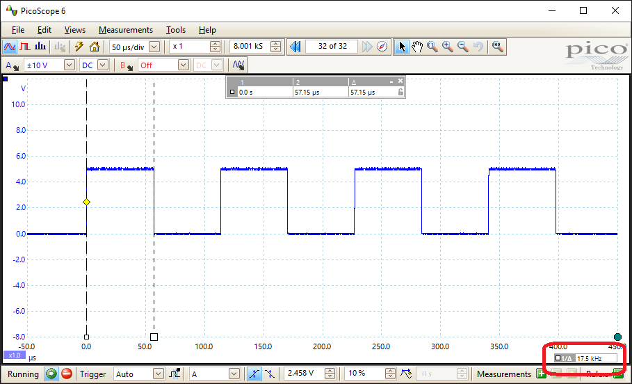
This trace measures A to D the conversions per second.
On each conversion, the PORTA bits were inverted so there were conversions on the rising and falling edges.
This gives about 17 500 samples per second. If your code needs to do other work, this rate would be slowed down.
Contact, Copyright, Cookies and Legalities: C Neil Bauers - reviseOmatic V4 - © 2016/17
Hosted at linode.com - London
Please report website problems to Neil