MOSFET |
|
To gain access to revision questions, please sign up and log in.
Metal Oxide Semiconductor Field Effect Transistor
Small changes in gate potential produce large changes in the current flowing from source to drain.
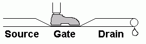
Here is a water analogy of a MOSFET. Pressure on the hose depletes the available water under your foot so the flow is cut off. The gate in the diagram below is your foot.
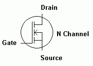
Field effect transistors are three pin devices. The pins are called the SOURCE, GATE and DRAIN. (Don't confuse these voltage controlled devices with bipolar transistors which are current controlled.)
This diagram shows an N Channel MOSFET. The insulation between the gate and the channel is very thin and easily destroyed by electrostatic discharge. Anti-static precautions need to be taken when handling MOSFETS.
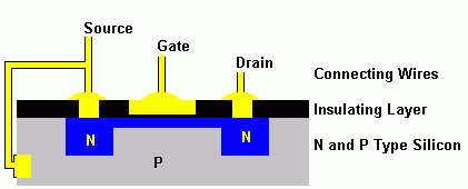
The gate potential causes an electric field in the gate region of the MOSFET. This potential alters the number of N Type carriers in the gate region.
P Channel MOSFETS are available too. They work in the same way but a negative potential causes enhancement.
reviseOmatic V3 Contacts, ©, Cookies, Data Protection and Disclaimers Hosted at linode.com, London