RANDOM PAGE
SITE SEARCH
LOG
IN
SIGN UP
HELP
To gain access to revision questions, please sign up and log in.
Everyone
aAtoms
- All matter is made of atoms.
- Atoms consist of a small positive nucleus surrounded by a cloud of negative electrons.
- Electrically neutral (not charged) matter has equal or balanced amounts of positive nuclei and surrounding negative electrons.
- Electrons are arranged around the nucleus in layers or shells. The outer shell is the important one for chemistry, electronics and semiconductor manufacturing.
- The animation shows a hydrogen atom with one proton and one electron. The particles are minute and the atom is mostly empty space.
bConductors
- These are materials where some of the electrons surrounding the atoms are free to move.
- Good conductors (all metals) have a very low resistance and many free electrons can move very easily. We usually assume the resistance is zero but in fact it is just very close to zero.
- Poor conductors (carbon is a good example and some metal alloys and oxides) have a few free electrons and they move much less freely. These materials are used in resistors.
cInsulators
- Insulators (plastic, wood and paper are good examples) have extremely few free electrons. They are all tightly bound to their parent atoms and they can't move. If the electrons can't move, current can't flow. There are examples of plastics where conducting materials have been added. These include anti-static plastic bags and foam rubber blocks.
dSemiconductors
- Pure (intrinsic) semiconductors (Silicon is the most common one) do not allow electrons to flow at room temperature.
- Silicon can be doped. This is the addition of controlled amounts of impurities.
- Doped silicon has interesting properties and many semiconductor devices with different properties can be manufactured.
- Each silicon atom has four electrons in the outer shell.
- In pure silicon, the outer electrons become free to move if the silicon is very hot. All the other electrons are always tightly bound to the nucleus.
- Beware: Silicone (with an E) is used for breast implants and bathroom sealants. It is never used in electronic circuits. It might be used to make a circuit box waterproof.
eDope

- This is the addition of tiny and carefully controlled amounts of impurities.
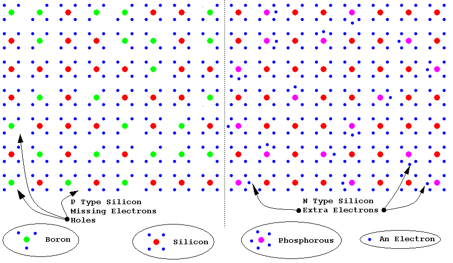
- N type silicon is doped with atoms that have five electrons in the outer shell. This means that there are extra electrons. These can flow at room temperature.
- P type silicon is doped with atoms that have only three electrons in the outer shell. This leaves holes where an electron would normally be expected. These holes can move at room temperature.
fSilicon doped with Boron and Phosphorous
- By fabricating devices with suitable zones of P and N type silicon, it is possible to manufacture the devices familiar to electronic engineers.
- The Diode has a PN junction. This is a layer of P type and a layer of N type silicon. The useful property is that current can only flow in one direction. You need to study quantum physics to really understand why this is. A layman's explanation is that electrons can flow into holes. If a potential difference is applied in the other direction, a region is created where there are no charge carriers so no current flows. This is called a depletion zone.

- The Bipolar NPN transistor has three layers of doped silicon. It is useful because a small base current can control a much larger collector/emitter current.
- Microchips are complex circuits built from many transistors all fabricated onto one silicon wafer. Many millions of devices can be deposited onto one wafer.
gVideos
Semiconductor Fabrication - 11 Minute Video
hSuperconductors
These are specialised materials that have zero resistance at very low temperatures.
Superconductor Model Train Video - 3 Minutes
reviseOmatic V3
Contacts, ©, Cookies, Data Protection and Disclaimers
Hosted at linode.com, London

![]()